Question
Why does the driver output change depending on the comparison pattern [LHZX] of the previous cycle?
Answer
Pattern and signal condition have the following five relationships.
-
The pattern symbol (WFC) operates as follows.
- WFC:“0”,“1”,“N”,“P”(driver pattern): a voltage is output from a driver and comparison does not perform.
- WFC:“L”,“H”,“Z”,“X”(comparator pattern): a voltage is not output from a driver and comparison performs.
-
The timing which changes from “Driver off” state to “Driver on” state is the time specified in [Driver On] in [Signal] tab. Once turned “Driver On” state, the driver will maintain to be “Driver On” state until the time specified in [Driver Off] of the subsequent comparator pattern cycle.
-
The timing which changes from “Driver on” state to “Driver off” state is the time specified in [Driver Off] in [Signal] tab. Once turned “Driver Off” state, the driver will maintain to be “Driver Off” state until the time specified in [Driver On] of the subsequent driver pattern cycle.
-
The logic state of the driver changes at the time of [Timing A] or [Timing B] in each cycle, and its state is maintained until the time of [Timing A] or [Timing B] of the next cycle.
-
The logic state of the driver also changes with the comparator pattern (WFC:“L”,“H”,“Z”,“X”).
- WFC:“L” : The logic state of the driver is “0”.
- WFC:“H” : The logic state of the driver is “1”.
- WFC:“Z” : The logic state of the driver is “N”.(*1)
- WFC:“X” : The logic state of the driver is “P”.(*1)
*1:For “N” and “P”, individual timing can be specified only when [Individual Timing Mode] in [Signal] tab is enabled. if it is disabled, “N” operates with “0” setting and “P” operates with “1” setting.
For example, if the pattern in “Pin1” will change from “X” to “0” on the following signal condition, 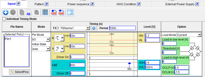
- the timing of [Driver On] is specified to “0s”.
- the timing of [Timing A] of cycle “0” is specified to “falling down at 50ns”.
since the logic state of the driver of “Pin1” is “1”(because [Individual Timing Mode] is disable), the driver output becomes the voltage value set to [VIH] after “0s”(specified in [Timing A]) when the pattern cycle is switched.
After that, according to the timing value of [Timing A] on cycle “0”, the driver output will become the voltage value set to [VIL] after “50ns”.
To avoid this phenomenon, set [Timing A] on cycle “0” and [Driver On] to the same value.